| Search for content and authors |
Laboratory of Scanning Electron Microscopy and X- ray Microanalysis at the Kielce University of Technology as research and industry support |
| Justyna M. Kasińska 1, Piotr Furmańczyk , Krzysztof Antoszewski |
|
1. Kielce University of Technology, Al. Tysiaclecia P.P.7, Kielce 25-314, Poland |
| Abstract |
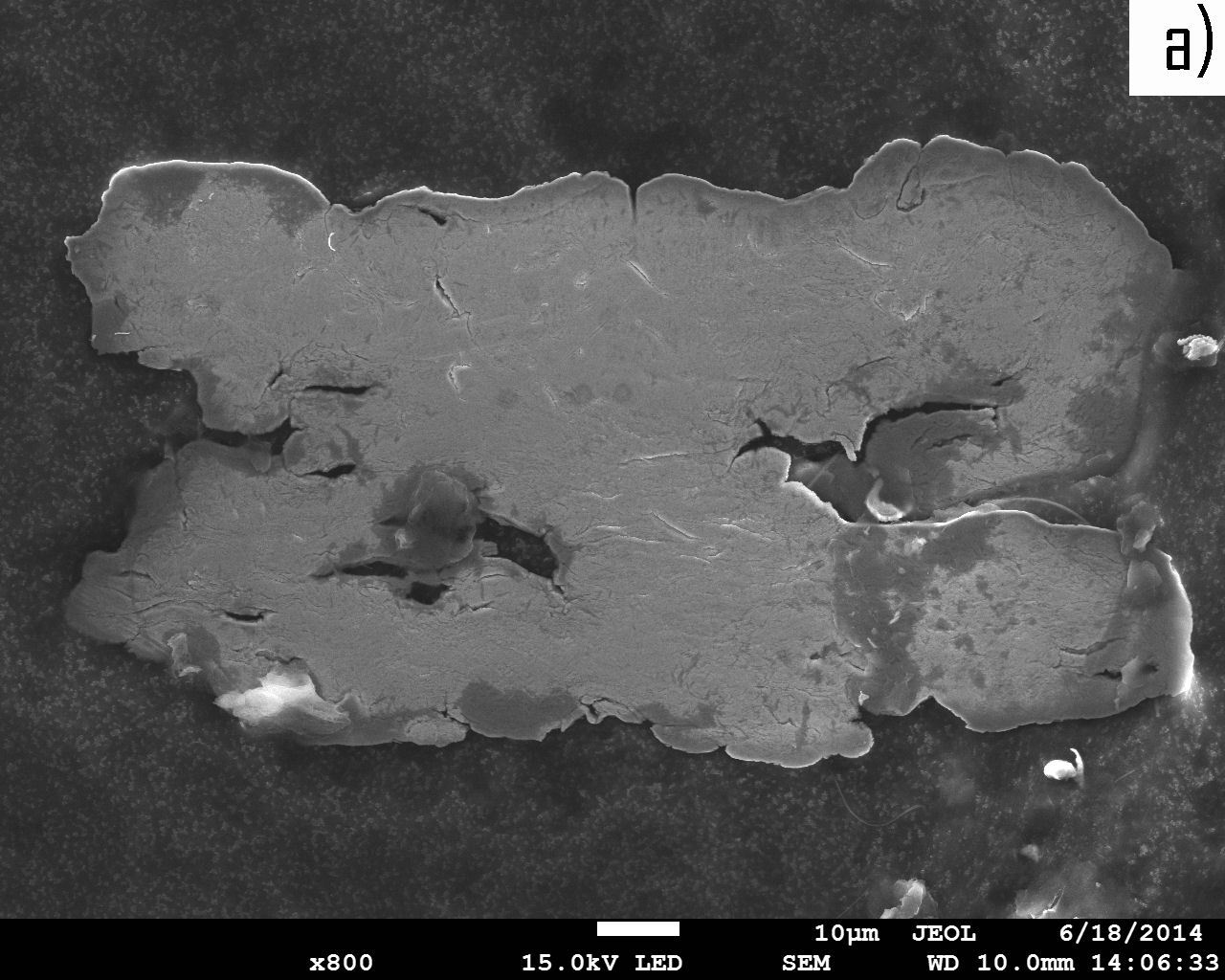
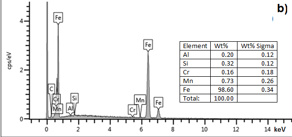
The development of microscopy is a direct result of advances in the technology of materials that have been observed for the last several dozen years. Relatively low resolving power of light microscopes contributed to the design of electron microscopic methods which enable the researchers to view nano- and sub-nano-sized objects. Modern transmission electron microscopes can easily resolve details of 0.05 nm. Introduction Today, the resolving power of scanning microscopes is approximately 1nm. The resolution of the produced image is directly related to the wavelength of electrons, which is a function of accelerating voltage used (the higher voltage the shorter wavelength and thus the better resolution), and to the diameter of the beam. One of the advantages of scanning electron microscopes is that they allow observations of certain surfaces without the need for them to be processed to produce a suitable sample. Kielce University of Technology purchased a modern JEOL JSM 7100F- scanning microscope in the framework of the project called “Developing research resources for specialized labs at public universities in the Świętokrzyskie region” co-financed from the European Fund for Regional Development under the “Innovative Economy” Operational Programme. The resolving power of the JEOL JSM 7100F is 1.2 nm, which allows the user to observe nanostructures. The observations at the Laboratory of Scanning Electron Microscopy and X-ray Microanalysis range from those with 25-fold magnification to 100 000x working magnification used to view objects with dimensions less than 20 nm. Contracted services. Representative SEM images. 1. Identification of contamination in the elements of parts of machinery. The analysis allows determining the chemical composition of the contamination.
Fig.1. Analysis of the chemical composition of the contamination; a) image of the contamination at 800x; b) EDS spectrum of the contamination. 2. Identification of non-metallic inclusions in a rolled member. The research led to the elimination of inclusions from the finished rolled members.
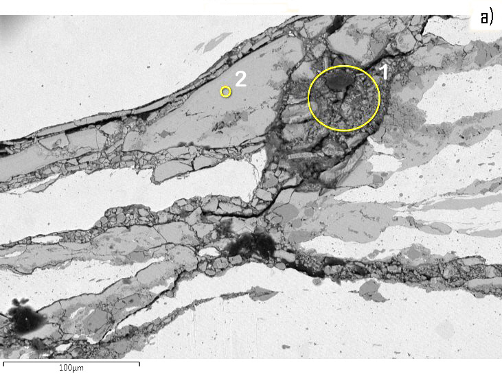
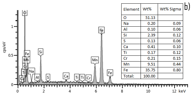
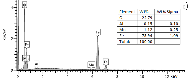
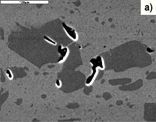
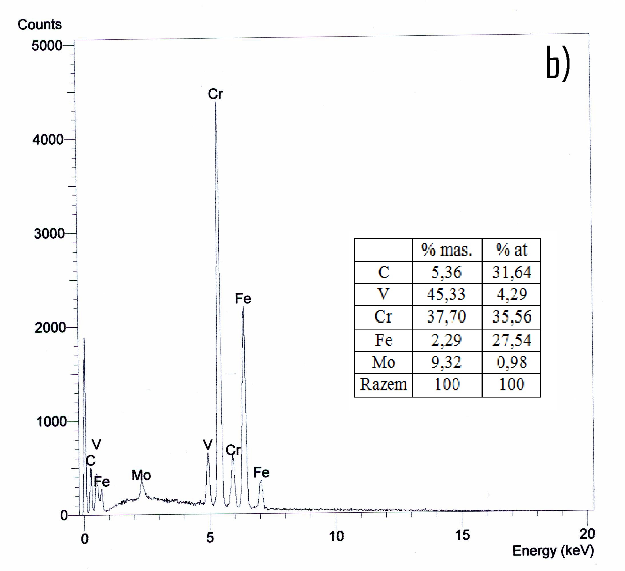
Fig.2. Analysis of non-metallic inclusion; a) non-metallic inclusion at 400x; b) EDS spectrum and chemical composition from the region marked as 1 in Fig. 2a; c) EDS spectrum and chemical composition from the region marked as 2 in Fig. 2a (EDS) 3. Identification of the causes of metallurgical flaws-related cracks in the matrix. Observations of microstructure and analyses of the matrix chemical composition allowed the detection of metallurgical defects, which were the major factor in initiating the crack.
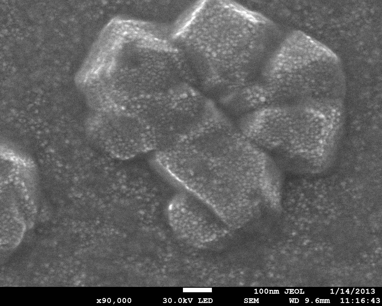
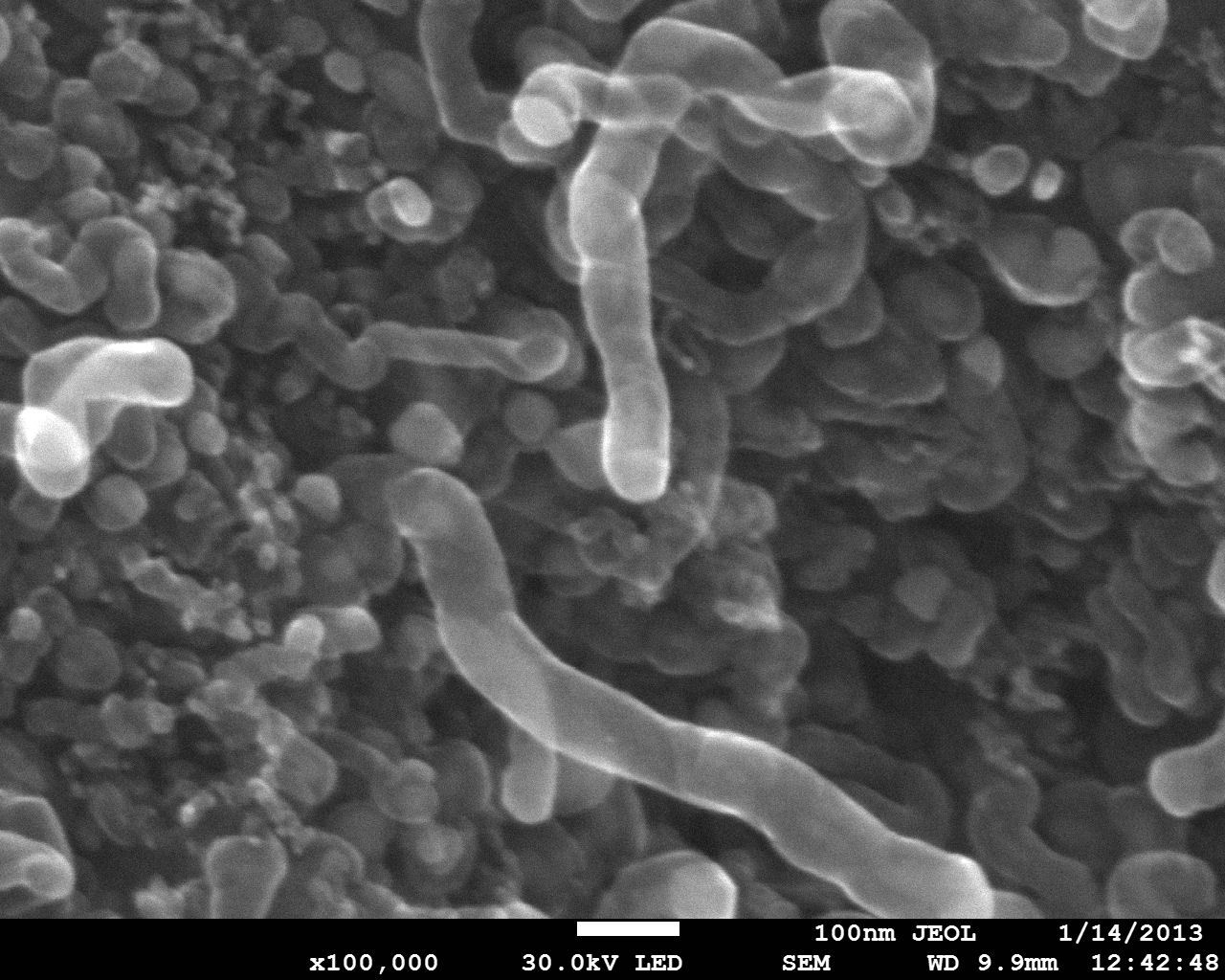
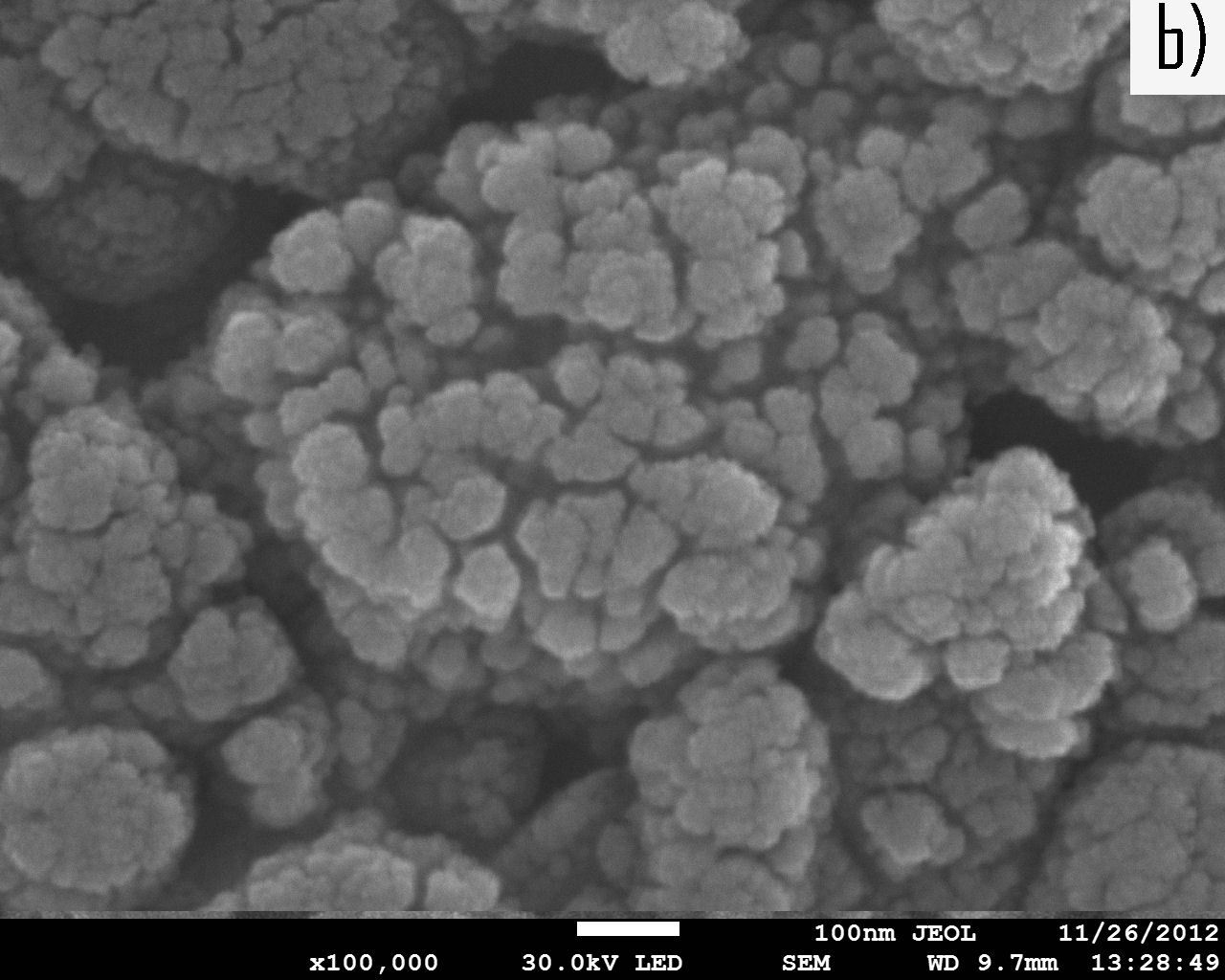
Fig. 3. Analysis of the inclusion; a) inclusion in the structure of the matrix material, unetched, 2 000x; b) EDS spectrum and the chemical composition of the inclusion in Fig. 3a. Research outcome, examples 1. Study of carbon-nickel nanolayers produced using physical vapour deposition (PVD) and the layers modified in the chemical deposition (CVD) process. The carbon-nickel layer on the sample is several hundred nm thick and consists mainly of fullerene C60 with an addition of nickel crystallites, Fig.4. In the process of chemical vapour deposition, carbon nanotubes form on the nickel crystallite embryos, Fig. 5. The layers investigated were produced at the Tele&Radio Research Institute, Warsaw by he research team headed by Prof. Elżbieta Czerwosz.
Fig 4. Carbon-nickel nanolayer prepared using physical vapour deposition (PVD) at 90 000x.
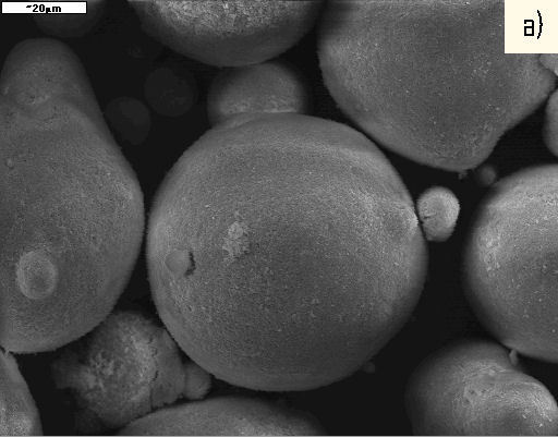
Fig. 5. Carbon-nickel nanolayer modified using chemical vapour deposition (CVD) – nanotubes at 100 000x. 2. Study of the morphology of Al2O3-13TiO2 nanostructured powder grains used in plasma spraying.
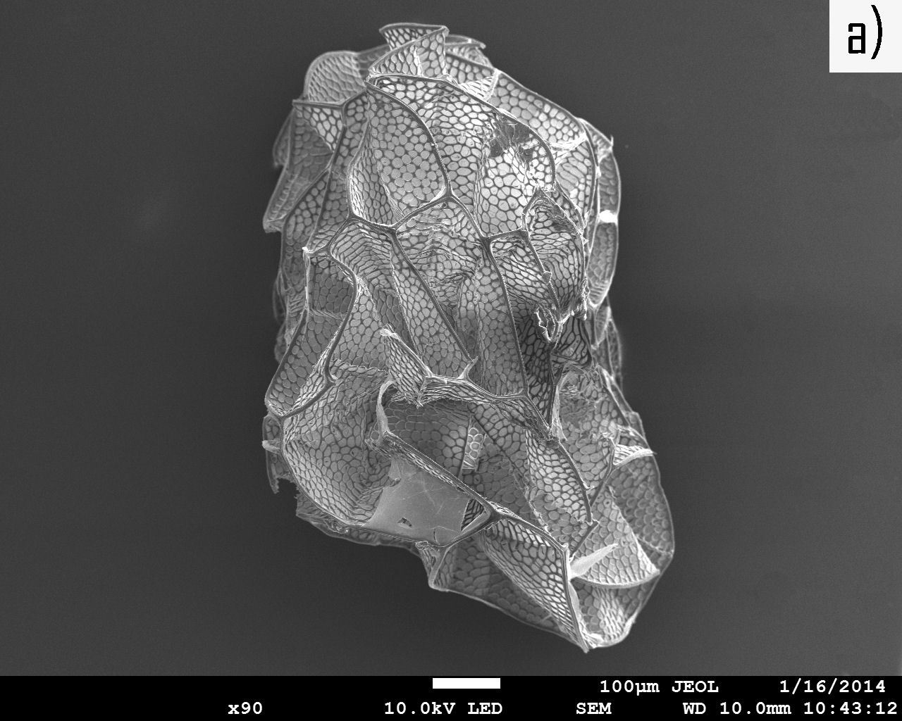
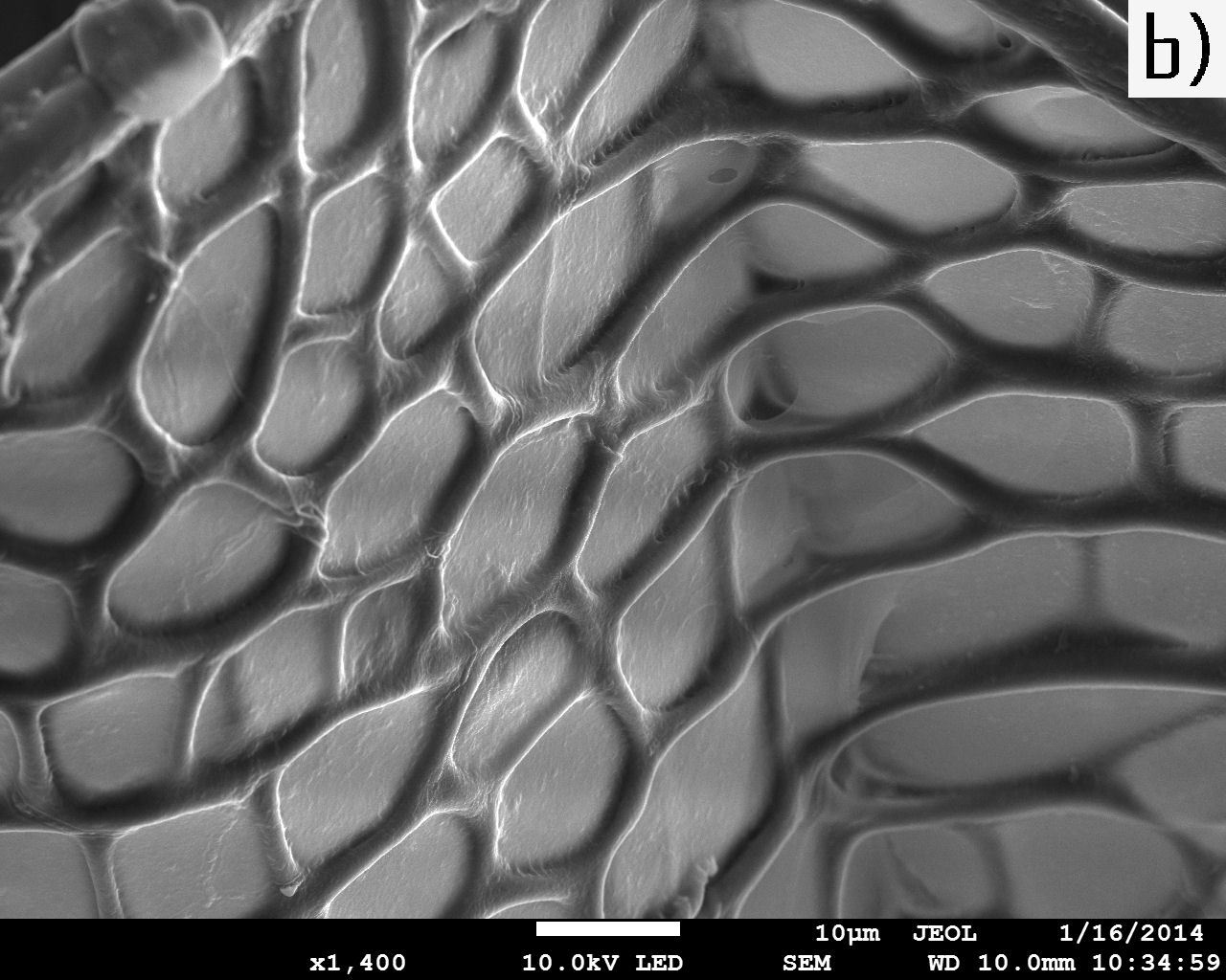
Fig. 6. Al2O3-13TiO2 nanostructured powder grain; a) image of a powder grain at 2 000x; b) image of the grain surface at 100 000x. 3. Testing biological samples. Dry samples are coated with a conductive layer of gold or carbon prior to being observed. Figure 7 shows a seed of Xylanche himalaica, a very rare plant from Fujiyama, Japan, parasitic on Rhododendron species 3000 m above sea level.
Fig. 7. A seed of Xylanche himalaica (Orobanchaceae) a) general image at 90x b) image of a seed wall at 1400x. Summary The Laboratory of Scanning Electron Microscopy X-ray Microanalysis at Kielce University of Technology provides analytical, research and developmental support for academic and industrial organizations. Typical applications include: - product quality control and the analysis of flaws in the form of cracks, non-metallic inclusions, corrosion, etc.; - evaluation of plastic forming, thermal and thermal-chemical treatment samples; material identification; - preparation of test specimens; - Vickers/micro and macro hardness measurements; - Investigations of non-metallic samples including ceramics, concrete and biological specimens. |
| Legal notice |
|
Presentation: Poster at Nano PL 2014, Symposium A, by Justyna M. KasińskaSee On-line Journal of Nano PL 2014 Submitted: 2014-06-30 05:28 Revised: 2014-09-29 08:40 |