| Search for content and authors |
Nano-inks for printing of electric circuits for microelectronic technology |
| Andrzej J. Mościcki 1, Anita K. Smolarek 1, Tomasz Fałat 2, Andrzej E. Kinart 1 |
|
1. Amepox Microelectronics, Ltd. (AMEPOX-MC), Jaracza 6, Łódź 90-268, Poland |
| Abstract | |||||||||||||||||||||||||||
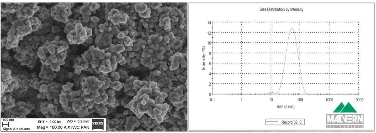
Actual microelectronic industry needs new and advanced materials and technologies for reason of miniaturization and very high reliability. Nano sized metals as silver or copper as a electrically conductive fillers gave possibility to develop new types of formulations called Nano Inks for packaging technologies and for making electrical circuits on rigid substrates and flexible polymer foils. The paper present information about possibility use of nano size silver for electronic packaging technologies. Each kind of ink, needs different nano silvers is shown in Fig. 1 and Fig. 2. 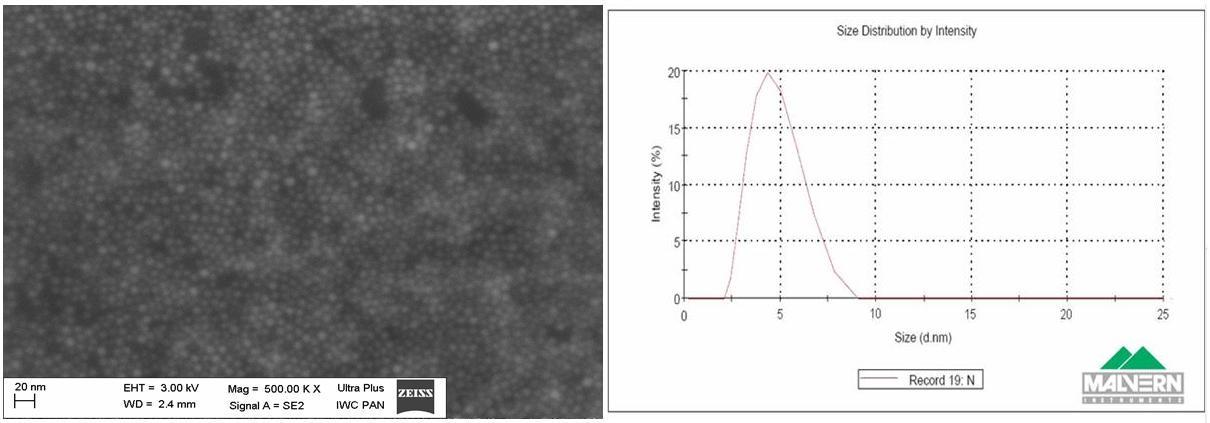
Figure 1. SEM picture of the smallest nanoAg and particle size distribution by “Malvern Zeta Sizer”.
Figure 2. SEM picture nanoAg and particle size distribution by “Malvern Zeta Sizer”. As it is well known, nanosized silver does not exist without protection layer around each particles. When metallic nanoparticle inks are heated the dispersants first, and protective layer the second, should be effectively removed allowing the remaining active metallic nanoparticles to be successfully sintered. We have tested several types of nanosilvers with different coating shells. Basing on Ag with paraffin and polymer coating the conductive inks were tested in Amepox lab. The base properties of the inks are shown in Table 1.
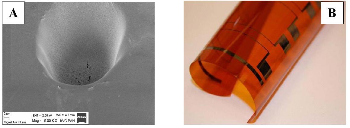
In this paper, we report on the basic properties of different inks, conditions for making printed stuctures and other possibilities as microvias interconnections (Fig.3).
Figure 3. A – Interconnection through microvia-hole by using ink. B – Printed structures on polymer foil. | |||||||||||||||||||||||||||
| Legal notice |
|
| Related papers |
Presentation: Invited oral at Nano and Advanced Materials Workshop and Fair, by Andrzej J. MościckiSee On-line Journal of Nano and Advanced Materials Workshop and Fair Submitted: 2013-06-25 13:43 Revised: 2013-06-25 13:43 |