| Search for content and authors |
Growth Methodologies for Overcoming the Perceived Limitations of Phase Separation and p-type Doping in InGaN |
| William A. Doolittle , Brendan P. Gunning , Chloe Fabien , Michael W. Moseley |
|
School of Electrical and Computer Engineering, Georgia Institute of Technology, Atlanta, GA 30332, United States |
| Abstract | ||
| While the InGaN material system is attractive for a wide variety of electronic and optoelectronic device applications, its potential is hindered by significant growth challenges such as p-type doping and the inability to grow thick, non-phase-separated films. Large background donor concentrations, particularly in high-indium composition InGaN, and the deep Mg acceptor level combine to make p-type doping above 1018cm-3very difficult. Simultaneously, InGaN films with indium fractions between 20% and 80% are notorious for phase separation where the film preferentially forms into discrete regions of varying indium composition rather than a single homogeneous alloy. More recently, a modified form of MBE called Metal-Modulated Epitaxy (MME) has shown the ability to overcome both of these challenges.
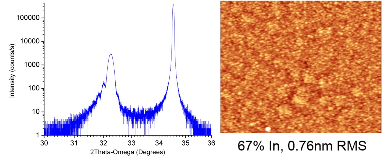
MME uses metal-rich fluxes, shuttering the metal sources while impingent nitrogen remains constant in order to consume any accumulated metal on the surface. This technique allows for lower substrate temperatures in order to facilitate the growth of high-indium content, non-phase-separated InGaN films. The samples here were grown well within the miscibility gap, from 22% to 67% indium fraction. Key growth considerations will be discussed in details, with a focus on transient RHEED analysis which plays a critical role in optimizing the InGaN growth chemistry. By monitoring the growth surface with RHEED, phase separation can be avoided without sacrificing crystal quality as is traditionally seen for nitrogen-rich growth. The InGaN films grown demonstrate GaN template-limited crystal quality with (0002) rocking curve FWHM less than 420 arcseconds in all cases, as well as smooth surfaces with less than 1nm RMS roughness. Figure 2 shows the XRD spectrum and AFM morphology for one such InGaN film with 67% indium fraction.
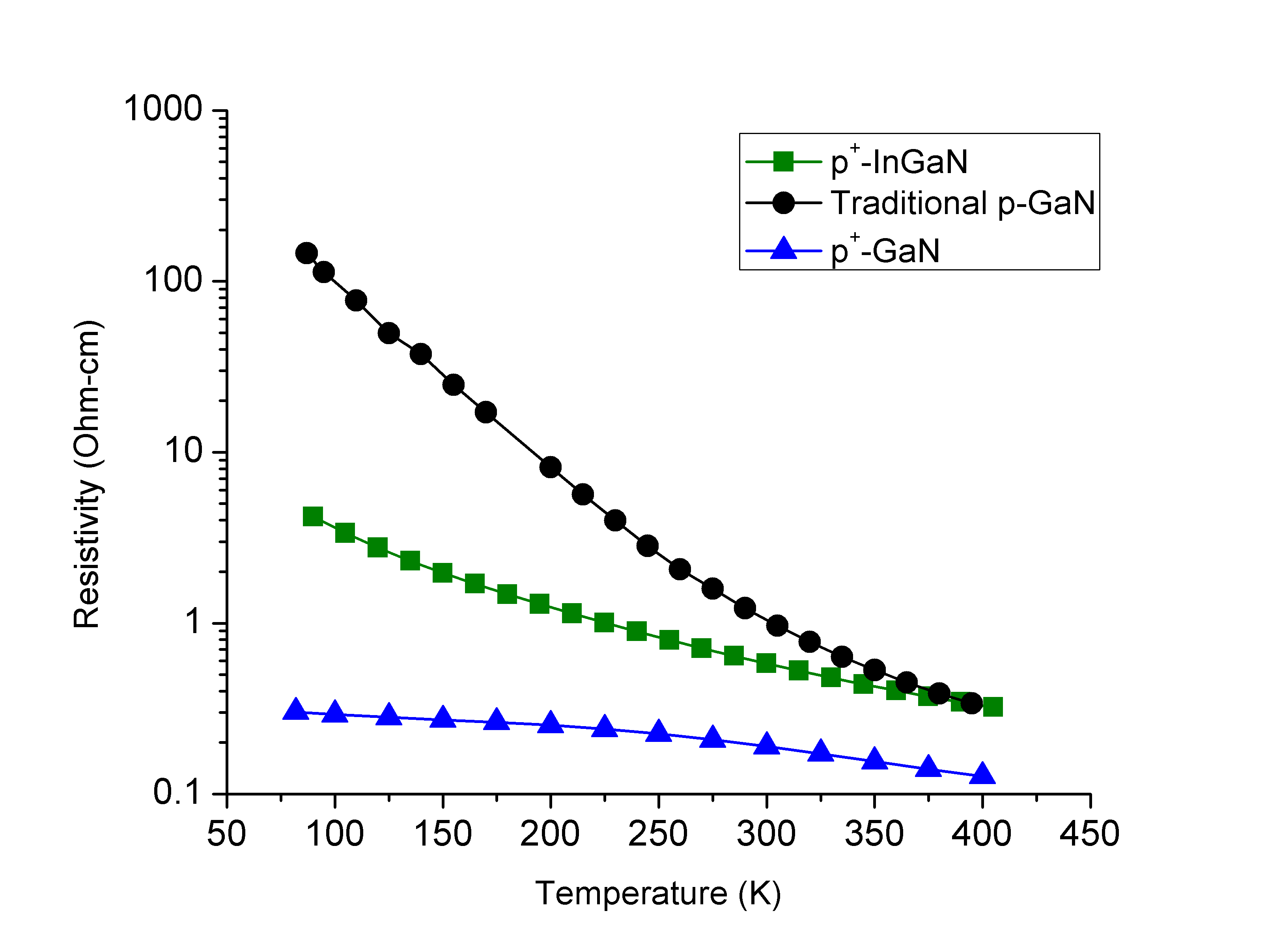
Figure 2.Temperature-dependent of resistivity of a traditional p-type GaN (black) which exhibits carrier freeze-out, compared to the highly-doped p+-GaN and p+-InGaN grown by MME. | ||
| Legal notice |
|
| Related papers |
Presentation: Invited oral at 17th International Conference on Crystal Growth and Epitaxy - ICCGE-17, General Session 10, by William A. DoolittleSee On-line Journal of 17th International Conference on Crystal Growth and Epitaxy - ICCGE-17 Submitted: 2013-05-31 13:11 Revised: 2013-07-19 22:23 |