| Search for content and authors |
GaN substrates with variable surface miscut for laser diode applications |
| Marcin Sarzynski 1, Robert Czernecki 1, Ewa Grzanka 1, Jaroslaw Domagala 2, Mike Leszczynski 1 |
|
1. Polish Academy of Sciences, Institute of High Pressure Physics (UNIPRESS), Sokolowska 29/37, Warszawa 01-142, Poland |
| Abstract |
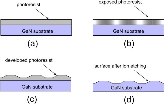
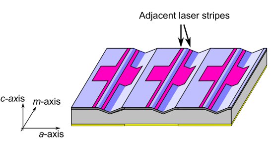
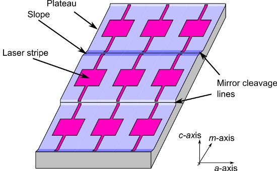
All modern GaN-based optoelectronic devices consist of a stack of epitaxial layers, with different chemical composition and thickness, grown on different kind of native or foreign substrates. In case of laser diodes (LDs), the substrate is always freestanding GaN, preferably with threading dislocation density not exceeding 106/cm2. For LD structure growth by MOVPE, the substrate crystal must not be exact oriented. Instead, a small off-cut (0.3-0.6 degree) of the surface is needed to maintain the step-flow growth mode. In case of III-nitride optoelectronic devices, the active region (most often quantum well structure) is made of the ternary compound, InGaN, and adding more indium to the compound lowers its bandgap from 3.5 eV for pure GaN down to about 0.9 eV for InN. Interestingly, for a fixed set of growth parameters (MOVPE), when the off-cut angle of the substrate is increrased, indium content in the layer decreases, respectively. This effect is also present when the off-cut angle is changed only locally (by special patterning technique), in several micrometer sized regions of the substrate. GaN substrates with differently angled regions can be fabricated using the well known technique for diffraction optics elements fabrication. In our case, it was special laser protholithography, capable of producing multilevel photoresist patterns, and ion etching, see Fig. 1. With this technique we were able to fabricate ridge-waveguide, edge emitting laser diodes with different amount of indium in the QWs (and emitting at different wavelengths) on a single substrate. In the present paper we will show how the local off-cut angle of the substrate influences LDs parameters such as the wavelength, threshold current and differential eficiency. We will also support the results by AFM and CL measurements. Next, we will show how the discussed substrate patterning technique could be used to obtain multiwavelength laser diode mini-arrays (see Fig. 2a.) and LDs with lower amount of indium near the mirror facet regions (Fig. 2b). In the latter case, we expect less light absorption, less heating and longer lifetime of high-power LDs.  Fig. 1. Process flow for fabrication of GaN substrate with variable off-cut angle. (a) Exact oriented GaN substrate with uniform photoresist layer, (b) photoresist exposed by a laser writer with variable light dose, (c) photoresist profile after development, (d) GaN profile after ion ething. 
(a) 
(b) Fig. 2. (a) Schematic of a laser diode mini-array. Due to different substrate off-cut (and different indium content of the active region), each stripe emits at a different wavelength. (b) Schematic of a single stripe laser diode with non-absorbing mirrors. Due to increased substrate off-cut near the mirror facets, the amount of indium is lower in those regions than in the laser stripe region. Thus, light emitted in the stripe region is not absorbed in the facet region. |
| Legal notice |
|
| Related papers |
Presentation: Oral at 17th International Conference on Crystal Growth and Epitaxy - ICCGE-17, Topical Session 3, by Marcin SarzynskiSee On-line Journal of 17th International Conference on Crystal Growth and Epitaxy - ICCGE-17 Submitted: 2013-04-15 15:02 Revised: 2013-04-15 15:43 |