| Search for content and authors |
Behavior of defects in a-plane GaN films grown by Low-Angle-Incidence Microchannel Epitaxy (LAIMCE) |
| Noriyuki Kuwano 1, Yuki Ryu 2, Masatoshi Mitsuhara 2, Chia-Hung Lin 3, Shota Uchiyama 3, Takahiro Maruyama 3, Yohei Suzuki 3, Shigeya Naritsuka 3 |
|
1. University of Technology Malaysia (UTM), Jalan Semarak, Kuala Lumpur 50400, Malaysia |
| Abstract |
Gallium nitride (GaN) grows usually in wurtzite structure (P63mc) that does not have the center of symmetry, and then it has the crystallographic polarity (thereafter called polarity). The polarity causes the piezoelectricity leading to the quantum-confined Stark effect. Since the wurtzite structure has the strong polarity along c<0001>, many efforts have been made so far to grow films along the direction other than c<0001>, such as non-polar direction m[01-10] or a[2-1-10] [1-4] and semi-polar direction normal to (11-22) or (1-101) [5-8]. Unfortunately, thin films grown in such directions usually contain a lot of lattice defects. In this work, a-plane GaN thin films were grown by a novel method of the "low-angle-incidence microchannel epitaxy (LAIMCE) " [9-10]. Cross sectional transmission electron microscope (TEM) observation was performed to analyze the behavior of lattice defects in order to clarify the effects of the present method on the growth of high-quality non-polar thin films. Special attention was paid to the difference in the behavior of defects between the wing-areas that grew along +c and -c directions. An a(2-1-10) plane GaN template with a stripe type SiO2 mask was prepared on a r(01-12) sapphire substrate. The mask had seed-windows of 3 μm wide and terraces of 7 μm wide. GaN was overgrown on the template by the metal-organic MBE using TMG and NH3 at 860ºC. The source gases were injected from the direction of +c[0001] of GaN. The injection angles were 5º for TMG and 45º for NH3. The polarity of GaN was distinguished from the difference in growth rate along c-direction under a certain growth condition (larger growth rate along +c direction). Thin foil specimens for TEM observation were made by using a focused-ion-beam (FIB) mill, followed by final finishing with an Ar+ ion mill. TEM characterization was carried out with a microscope of JEM-2000EX at accelerating voltage of 200 kV. The polarity of GaN was also confirmed from the relationship between the +c direction of wurtzite structure and the direction of c-axis of the r-plane sapphire substrate [11]. Burgers vectors B of lattice defects were analyzed by the conventional gB method.
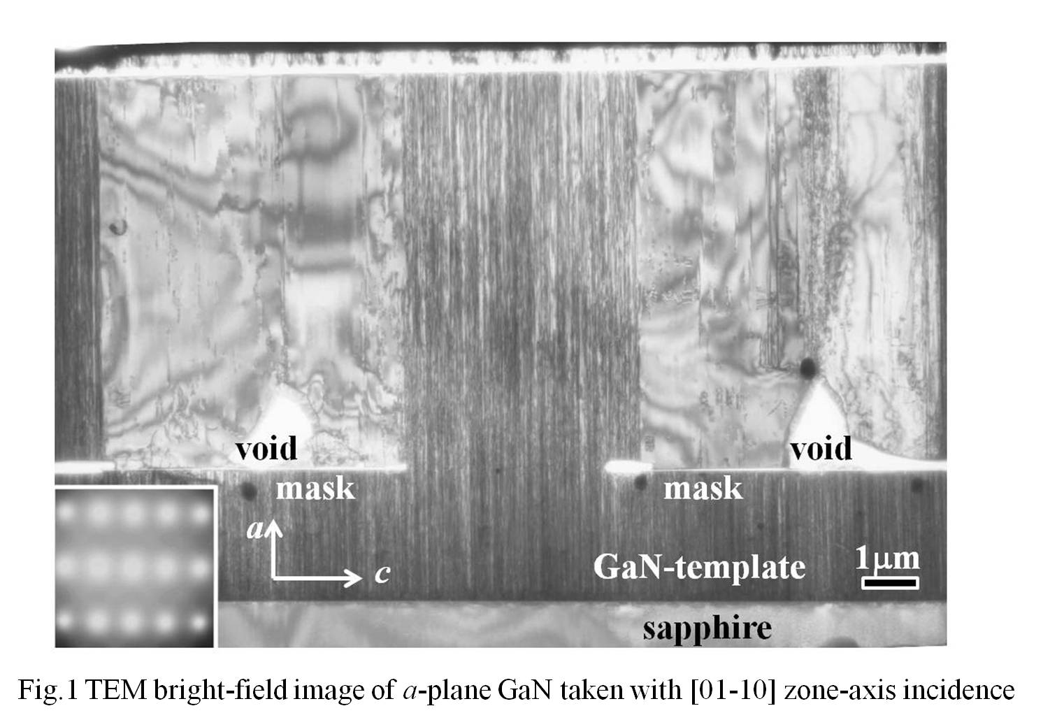
Figure 1 shows a TEM micrograph of a-plane GaN grown by the present method. The micrograph was a bright field image taken with [01-10] zone-axis incidence. It is clearly seen that the overgrown thin film has a very smooth and flat surface of a-plane. The GaN template contains a large density of threading dislocations (TDs), and some of the TDs propagate through the seed-windows, running straight up to the top-surface of the overgrown thin film. The density of TDs in the GaN template was roughly estimated to be of the order of 1010 cm-2, and the region in the overgrown layer has almost the same dislocation density over the seeding windows. From the gB characterization, most of the TDs were confirmed to be of (a+c) type. As these TDs do not bend in the overgrown layer, there are regions without TDs on the mask-terraces. The dislocation density is estimated to be less than 2 x 108 cm-2 at most. Inside the overgrown GaN thin film, a large void and small ones remain on the center and the ends of mask-terrace, respectively. The large voids are thought to remain on the terrace of mask after the wing regions coalesce with each other. As the large void is located at the center of terrace, the growth rates at +c and -c direction were almost the same as each other under the present growth condition. In other words, the regions of right-hand side and left-hand side are formed by the growth along -c and +c, respectively. One can see faint image-contrasts in the both wing regions over the mask-terraces. They are due to lattice defects that have been formed during the lateral growth of GaN. When the incident beam of TEM was parallel to [1-100], stacking faults (SFs) on the basal plane usually cannot be observed. By observation after tilting the TEM specimen, it was found that the both wing regions contain SFs on the basal planes. In c-plane GaN layers grown by the conventional way, there are scarcely such SFs. This suggests that the growth process of the wing regions is different from the case of conventional c-plane growth in spite that the wing regions were thought to be formed also by the c- plane growth at the early stage. We performed further TEM observation with different conditions in order to reveal the microstructure in the regions over the mask-terraces. Behavior of basal stacking faults and the effects of +c/-c growth direction on the lattice defects was discussed. A new method for a high quality GaN layer is proposed. References [1] F. Wu et al.: J. Appl. Phys., 94, 942 (2003). [2] Z. Lilietan-Weber et al.: Opto-Electr. Rev., 12, 339 (2004) [3] M. Araki et al.: Jpn. J. Appl. Phys., 47, 119 (2008) [4] N. Kuwano et al.: Phys. Stat. Sol., C6(52), S494 (2009) [5] A. E. Romanov et al.: J. Appl. Phys., 100, 023522 (2006). [6] H. Masui et al.: IEEE Trans. Electr. Device, 57, 88 (2010). [7] Z. H. Wu et al., Appl. Phys. Lett. 98, 051902 (2011). [8] T. Kuwahara et al., Phys. Stat. Sol., C9(3/4) 488 (2012). [9] G. Bacchin et al. J. Cryst. Growth 208, 1 (2000). [10] C-H. Lin et al.: J. Cryst. Growth, 318, 446 (2011). [11] J. K. Liu: J. Appl. Phys. 46, 3703(1975). |
| Legal notice |
|
| Related papers |
Presentation: Oral at 17th International Conference on Crystal Growth and Epitaxy - ICCGE-17, General Session 7, by Noriyuki KuwanoSee On-line Journal of 17th International Conference on Crystal Growth and Epitaxy - ICCGE-17 Submitted: 2013-04-15 14:50 Revised: 2013-04-15 15:35 |