| The interest paid to the heteroepitaxy of GaAs on Si has never failed in the last years due to the potential for monolithic integration of GaAs-based optoelectronic devices with Si integrated circuits (OEICs)[1]. However, three major problems remain unresolved in GaAs layers grown directly on plain silicon substrates, i) the high density of threading dislocations due to the large lattice mismatch with Si (around 4%), ii) the formation of anti-phase domains due to the presence of polar/non-polar interfaces and iii) the formation of cracks due to the difference in thermal expansion coefficients between the two materials[2]. Significant improvements have been reported for many years, thanks to selective area epitaxy (SAE) of GaAs on Si substrates patterned with dielectric film[3-6]. These problems have been overcome, for the case of Ge on Si hetero-epitaxy, and we have previously demonstrated defect free Ge regions grown on thin SiO2 layer where the crystalline order between epi-Ge and Si substrate was transferred through nano-holes in the SiO2 layer[7].
Besides, to demonstrate compatibility with the Si CMOS technology platform, growth temperature should be preferably limited to a maximum of 600°C. That was achieved, in our growth process, by the use of tertiarybutylarsine (TBAs) instead of AsH3 which has a higher cracking temperature. Thus, such epitaxy step could be added at any time in a CMOS process without degrading preexisting MOS device elements.
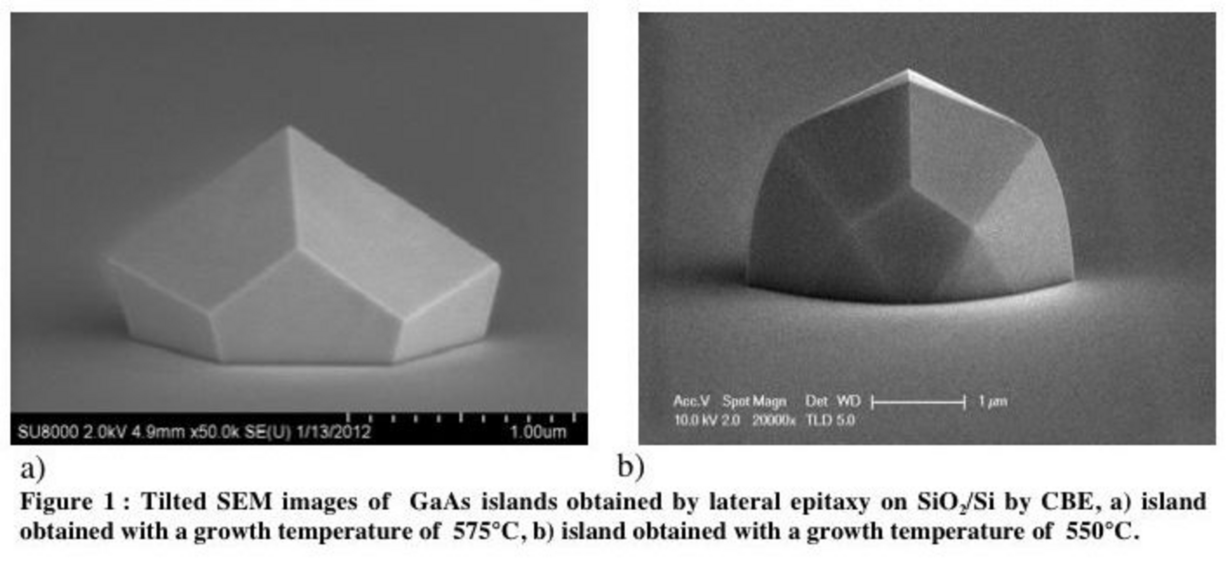
In this work, GaAs crystals were obtained by epitaxial lateral overgrowth (ELO process) directly grown on Si substrates at low temperature (ranging from 550 to 600°C) by chemical beam epitaxy (CBE). The investigated approach consisted in growing the GaAs layer from Si nanoscale seeds opened through a 0.6 nm thick SiO2 layer chemically formed on (001) and (111) Si substrate. The use of a sufficiently small nucleation area is expected (i) to enable the relaxation of the mismatched material without emission of misfit dislocations[8] and (ii) to avoid the formation of steps and therefore to result in a perfect alignment of group III or group V elements at the interface between Si and GaAs within the seed area.
Coherent growth without misfit dislocation and antiphase domain formation was confirmed at the hetero interface of GaAs islands and Si substrate for small width openings. The density of initial seeds islands was choosen low enough to avoid any coalescence, which is assumed to result in additional defects, but the resulting islands are large enough to serve as a possible III-V plateform in CMOS or optoelectronic integrated circuit processings.
This technique allows us to obtain perfect integration of heterogeneous GaAs islands of microscopic size through a Si substrate (Figure 1). The analysis performed on these 3D objects by X-ray diffraction (XRD) and transmission electron microscopy (TEM) indicate that GaAs islands are perfectly relaxed and in epitaxial relation with the Si substrate. Additional measures performed by confocal Raman microscopy on these islands help us to determine different structural parameters, such as stress induced during growth, chemical compounds, doping, crystalline quality and the presence of defects. Finally, the micro-photoluminescence (µ-PL) measurements allow us to probe precisely the discrete electronic states and to give information on the quality of surface interfaces.
These different results will be presented and discussed during the communication.
Reference :
[1] R. Chau, S. Datta, M. Doczy, B. Doyle, B.Jin, J. Kavalieros, A. Majumdar, M. Metz, and M. Radosavljevic, IEEE Trans. Nanotechnol. 4, 153 (2005)
[2] S. F. Fang, K. Adomi, S. Iyer, H. Morkoc, H. Zabel, C. Choi, N. Otsuka, J. Appl. Phys. 68, R31 (1990)
[3] J. Z. Li, J. Bai, J.-S. Park, B. Adekore,K. Fox, M. Carroll, A. Lochtefeld, Z. Shellenbarger, Appl. Phys. Lett. 91, 021114 (2007)
[4] J. Z. Li, J. Bai, C. Major, M. Carroll, A. Lochtefeld, Z. Shellenbarger, J. Appl. Phys. 103, 106102 (2008)
[5] M. Deura, T. Hoshii, M. Takenada, S. Takagi, Y. Nakano, M. Sugiyama, Journal of Crystal Growth 310, 4768 (2008)
[6] C.-W. Hsu, Y. -F. Chen, Y. -K. Su, Appl. Phys. Lett. 99, 133115 (2011)
[7]M. Halbwax, C. Renard, D. Cammilleri, V. Yam, F. Fossard, D. Bouchier, Y. Zheng and E. Rzepka, J. Crystal Growth 308 26 (2007)
[8]S. Luryi, E. Suhir, Appl. Phys. Lett. 49, 140 (1986)
|