Nanowires (NWs) made of GaN and related group III-N alloys, having a huge potential for new devices, attract much attention recently. The GaN-based materials are very thermally and chemically stable. This makes them very suitable for operation in chemically harsh environments. Therefore, wide band-gap group III nitride compound semiconductors are alternative options to supplement silicon, in particular in chemical sensor applications [1].
The aim of this paper is to report on our developments in plasma-assisted MBE growth of GaN NWs on Si(111) substrates and on their application in gas sensors. Two types of growth procedures were used to prepare GaN NWs structures. The first one, standard catalyst-free MBE growth at N-rich conditions, resulted in a dense ensemble of GaN NWs being ~400 – 500 nm long with diameter of 20 – 30 nm (see Fig. 1). They were homogenously distributed and well oriented with the c-axis being perpendicular to the substrate. Density of nanowires was quite large. Therefore, even a small tilt of some of them, estimated from XRD to be below ±2o, led to a partial coalescence in upper parts of NWs. In the second procedure, after growth of ~1 µm long NWs the conditions were changed to Ga-rich by increasing the Ga flux and reducing growth temperature. As the result the NWs were overgrown with a planar GaN layer (see Fig. 2).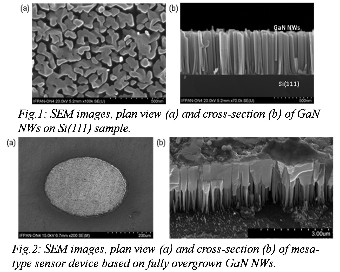
Two types of GaN NWs based gas sensors were fabricated. For the planar device samples with ensemble of GaN NWs grown on semiinsulating Si(111) substrates were used. Then, Ti/Al/Au electrical contacts having diameters of 400 µm were defined on the surface by standard photolithography and lift-off processes and annealed to form low resistance source and drain electrodes. Since NWs were closely packed thin bridges connecting them were created in the active area of the device between the electrodes. In vertical sensor devices electrical resistivity along the NWs, not across the NWs as in a planar geometry, is measured. In such a case, we used conductive Si substrate and overgrowth of NWs with a compact GaN layer. Then, a mesa-type sensors were made by dry etching and metal deposition techniques.
Finally, both types of structures were electrically tested in NO2, NH3 and hydrogen atmospheres at temperatures up to 80 oC to check and compare their gas sensing properties.
This work was partly supported by the European Regional Development Fund through grant Innovative Economy (POIG.01.01.02-00-008/08 NanoBiom). Some of us (MS and TP) are grateful for support from the POIG.01.03.01-00-159/08 Project.
[1] S.J. Pearton, et al., Prog. Mat. Sci. 55, 1-59 (2010); |