| Search for content and authors |
Hybrid optimization approach to modelling of semiconductor nanostructure and devices |
| Yiming Li |
|
Department of Communication Engineering, National Chiao Tung University, 1001 Ta-Hsueh Road, Hsinchu 00300, Taiwan |
| Abstract |
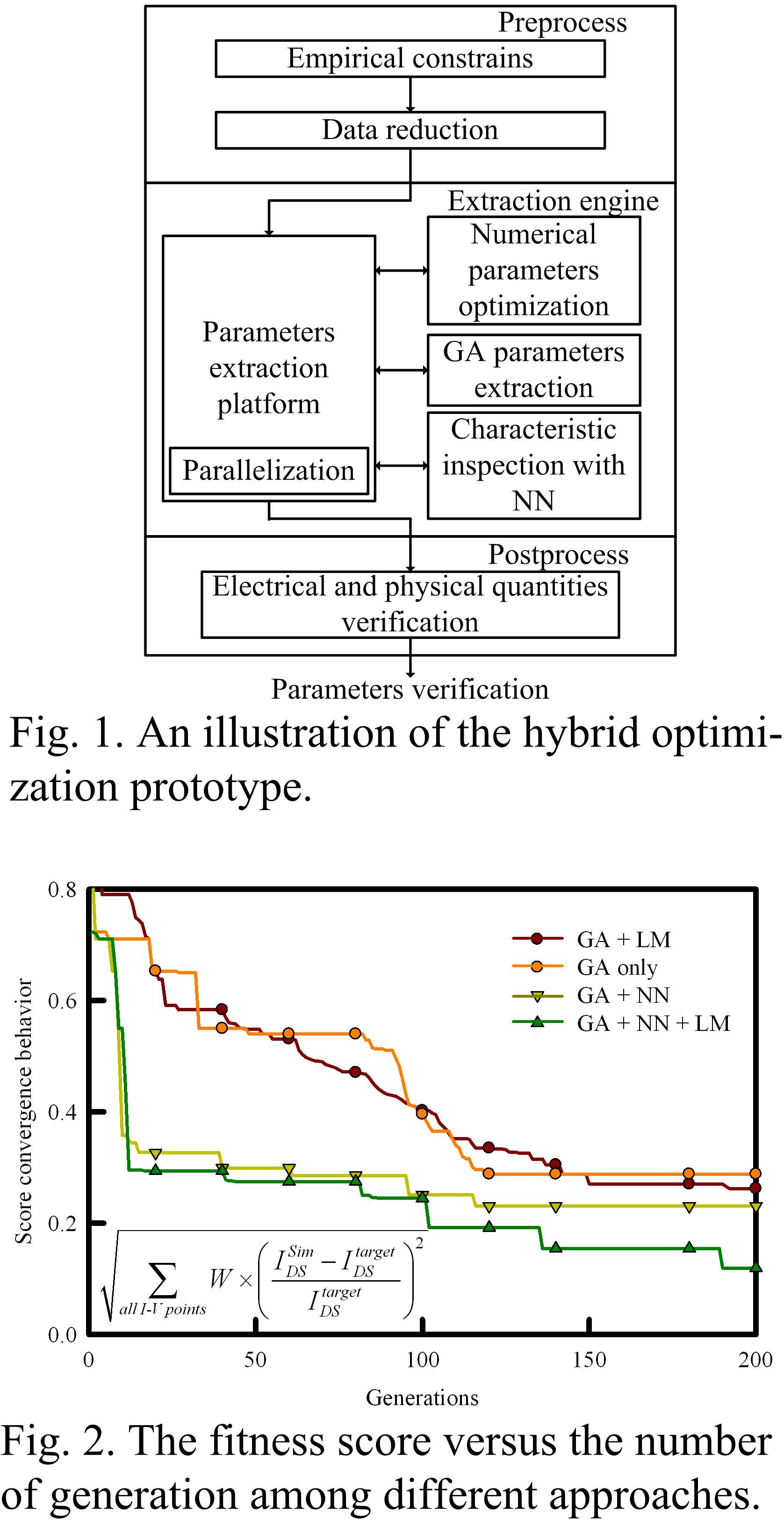
Model and optimal parameters have been at the heart of CAD tools for semiconductor technology over the past decades. Equivalent circuit models continuously play an active role in bridging the nanoscale device fabrication technology and IC design. As the mainstream CMOS technology is scaled into the nanoscale regime, hundreds of parameters have to be optimized and extracted for the corresponding model equations. Conventional manual adjustment is a bottleneck for advanced semiconductor materials and nanodevices. In this work, we present an intelligent parameter extraction technique for nanoscale semiconductor device and nanostructures; in particular, for sub-100 nm CMOS transistors. Based on the multiobjective distributed genetic algorithm, advanced numerical methods, adaptive neural network scheme, parallel computing techniques, and physical-based empirical rules, a hybrid approach, shown in Fig. 1, has been developed and implemented. Suppressing those difficulties of the conventional methods, the approach automatically mimics engineer’s rules to extract and optimize a set of parameters, in a global sense, for tens of transistors on a single wafer simultaneously. For the 90/65 nm CMOS technology, this window-based prototype demonstrates its capability to automatically extract the optimal parameters from several sets of measured I-V curves of more than 16 fabricated MOSFETs. Preliminary performance of the prototype is examined, as shown in Fig. 2. Applications of this intelligent extraction system in DC, AC, and RF parameters optimization for, such as CMOS, TFT, HBT, SOI, OLED, and power JEFT, have also been achieved. Besides, optimal electronic structure design of InAs/GaAs semiconductor quantum dot, ring, and molecules is further advanced by integrating a simulation-based technique in the prototype for energy state calculation. Semiconductor scientists and engineers would be very interested in this system.
 |
| Legal notice |
|
Presentation: Invited at E-MRS Fall Meeting 2007, Symposium G, by Yiming LiSee On-line Journal of E-MRS Fall Meeting 2007 Submitted: 2007-06-22 13:38 Revised: 2009-06-07 00:44 |